How to Fabricate Microfluidic Chips with Femtosecond Laser
A High‑Precision, Single‑Step Approach for Lab‑on‑a‑Chip Development
Introduction: The Microfluidics Fabrication Challenge
Microfluidic chips — often called lab‑on‑a‑chip (LOC) devices — have revolutionised biomedical research, chemical analysis, and point‑of‑care diagnostics. By manipulating fluids at the sub‑millimetre scale, these chips enable faster assays, lower reagent consumption, and higher throughput.
However, microfluidic chip fabrication remains a significant bottleneck for many research teams and prototyping labs. Traditional methods are either time‑consuming, expensive, or limited in design flexibility — especially when working with hard materials like glass or when rapid iteration is required.
This is where femtosecond laser micromachining for microfluidics offers a breakthrough. In this guide, we will walk through common fabrication approaches, explain why femtosecond lasers outperform conventional techniques, and provide a step‑by‑step workflow for producing high‑quality microfluidic chips.
Common Microfluidic Chip Fabrication Methods
Before diving into laser‑based techniques, it is useful to understand the existing landscape. The three most widely used lab‑on‑chip fabrication methods are:
1. Photolithography (Soft Lithography)
Process: A photomask is used to pattern a photoresist layer on a silicon wafer, followed by PDMS (polydimethylsiloxane) casting and bonding.
Advantages: High resolution (down to ~1 µm), well‑established.
Limitations: Requires a cleanroom; photomask fabrication is costly and time‑consuming; design changes need a new mask; primarily suited for PDMS, not glass.
2. CNC Micromilling
Process: A rotating micro‑endmill physically removes material from a substrate.
Advantages: No mask required; works with plastics and metals.
Limitations: Limited to feature sizes >50 µm; tool wear; mechanical stress can cause micro‑cracks; difficult to machine glass; debris and burrs require post‑processing.
3. CO₂ / Nanosecond Laser Ablation
Process: A pulsed laser (microsecond or nanosecond duration) vaporises material.
Advantages: Maskless; faster than CNC.
Limitations: Significant heat‑affected zone (HAZ) leads to melting, recast, and micro‑cracks — especially problematic for transparent materials like glass and for achieving smooth channel walls.
Why Femtosecond Laser? The Ultrafast Advantage
Femtosecond laser micromachining for microfluidics operates on an entirely different physical principle. With pulse durations in the 10⁻¹⁵ second range, the laser energy is deposited so rapidly that material transitions directly from solid to vapour — without melting.This leads to several critical benefits for microfluidic chip fabrication:
Feature Femtosecond Laser Nanosecond Laser / CNC Heat‑Affected Zone (HAZ) Negligible (sub‑µm) Significant (tens of µm) Edge Quality Smooth, crack‑free Rough, possible micro‑cracks Material Versatility Glass, PDMS, polymers, silicon, metals Limited for hard/brittle materials Aspect Ratio High (up to 50:1) Moderate Internal Channel Fabrication Yes (3D subsurface) No Post‑Processing Minimal or none Often required Key takeaway: For applications requiring smooth channel walls, high aspect ratios, or glass‑based microfluidics, femtosecond laser is the superior choice.
Step‑by‑Step: Fabricating Microfluidic Chips with Femtosecond Laser
The following workflow is typical for producing a microfluidic chip using our laser platforms at YMJ Optical.
Step 1: Design the Channel Network
Use CAD software (e.g., AutoCAD, SolidWorks, or layout‑specific tools like CleWin) to design the microchannel geometry.
Design considerations:
Channel width: 20 µm – 500 µm (depending on application)
Channel depth: 20 µm – 300 µm
Feature resolution: down to 5 µm
Include inlet/outlet ports and alignment marks for bonding.
Export format: DXF, DWG, or STEP.
Step 2: Material Selection
Material Suitability for Femtosecond Laser Typical Applications Glass (soda‑lime, borosilicate, fused silica) Excellent High‑temperature, chemical‑resistant, optical detection chips PDMS Good (via ablation of mould or direct writing) Rapid prototyping, cell culture, soft lithography masters PMMA / COC / COP Excellent Disposable chips, high‑volume production Silicon Excellent Integrated electronics + fluidics Step 3: Laser Micromachining (YMJ Platform)
At YMJ Optical, we use a high‑precision femtosecond laser system equipped with:
Pulse duration: <350 fs
Wavelength: 1030 nm (or 515 nm for finer features)
Scanning stage: High‑speed galvo + linear motor stage
Resolution: ±5 µm positioning accuracy
Process parameters (example for glass):
Parameter Typical Range Laser power 0.5 – 5 W (depending on material) Scan speed 50 – 500 mm/s Number of passes 1 – 10 (for deeper channels) Pulse energy 1 – 20 µJ The laser directly ablates the microchannel pattern into the substrate — no photomask, no cleanroom, no chemical development.
Step 4: Post‑Processing (Optional)
Cleaning: Ultrasonic bath in deionised water or isopropanol to remove ablation debris.
Annealing (for glass): 500 °C for 2 hours to relieve residual stress (often not required with optimised parameters).
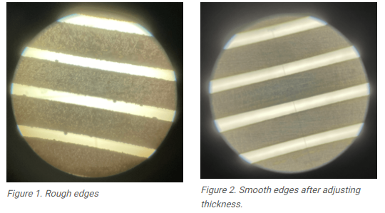
Polishing: Not necessary for most applications due to the inherent smoothness of femtosecond‑ablated surfaces (Ra < 0.3 µm).
Step 5: Sealing / Bonding
To form enclosed channels:
Glass‑to‑glass: Thermal bonding (clean surfaces, 600 °C, 4 hours)
Glass‑to‑PDMS: Plasma treatment followed by conformal contact
Polymer‑to‑polymer: Solvent or thermal bonding
Inlet/outlet ports can be drilled using the same femtosecond laser or a dedicated drilling step.
Materials Deep Dive: Glass, PDMS, and Polymers
Glass Microfluidics
Why choose glass: Optical transparency, chemical inertness, high thermal stability, low autofluorescence.
Femtosecond advantage: Traditional glass machining requires wet etching (dangerous chemicals) or picosecond lasers (higher HAZ). Femtosecond laser produces smooth, crack‑free channels directly.
YMJ capability: Soda‑lime, borosilicate (e.g., Schott D263), fused silica (e.g., Corning 7980).
✅ PDMS Microfluidics
Why choose PDMS: Gas permeability, biocompatibility, low cost.
Femtosecond advantage: Can directly ablate PDMS or — more commonly — ablate a metal or polymer master mould for PDMS casting, achieving µm‑scale features without a photomask.
✅ Polymer Microfluidics (PMMA, COC, COP)
Why choose polymers: Disposable, low‑cost, suitable for mass production.
Femtosecond advantage: Minimal thermal damage preserves optical clarity; high throughput via multi‑layer processing.
YMJ Solution: Equipment, Capability, and Case Example
Our Femtosecond Laser Micromachining Platform
Specification Value Laser type Femtosecond fibre laser Pulse duration <350 fs Wavelength 1030 nm / 515 nm (optional) Maximum power 20 W Minimum feature size 5 µm Positioning accuracy ±5 µm Working area 300 mm × 300 mm (expandable) Materials Glass, PDMS, PMMA, COC, COP, silicon, metals Case Example: Glass Microfluidic Chip for Cell Sorting
Customer: University biomedical engineering lab
Material: Borosilicate glass, 500 µm thickness
Channel width: 50 µm
Channel depth: 100 µm
Total chip size: 20 mm × 20 mm
Turnaround time: 3 working days from CAD file to sealed chip
Outcome: Successful particle focusing and cell sorting without channel clogging or optical distortion
Frequently Asked Questions (FAQ)
Q1: Can femtosecond laser fabricate 3D microfluidic channels inside glass?
Yes. By focusing the laser inside the glass substrate, we can create subsurface channels (without surface opening) — a unique capability not possible with CNC, photolithography, or nanosecond lasers.
Q2: How smooth are femtosecond‑ablated channel walls?
Typically Ra < 0.3 µm for optimised parameters, comparable to wet‑etched glass and significantly smoother than nanosecond‑laser or CNC‑machined surfaces.
Q3: Do you offer prototyping services for academic labs?
Yes. YMJ Optical provides low‑volume prototyping (1–50 chips) with fast turnaround. No photomask or tooling costs.
Q4: What file formats do you accept?
DXF, DWG, STEP, Gerber, or even hand‑sketched PDFs — we will work with your design.
Call to Action: Request Sample Processing
Ready to see how femtosecond laser micromachining for microfluidics can accelerate your research or product development?
Request a sample processing on your material
Receive a design review and fabrication quote
Discuss high‑volume manufacturing pathways
Request Sample Processing →
Include your CAD file or channel specifications, and we will respond within 24 hours