Precision Laser‑Cut Stencils for Prototyping to Production
Introduction
Frameless stencils are essential tools in modern electronics manufacturing. They are used for applying solder paste, flux, and solder balls to printed circuit boards (PCBs), wafers, and components — serving applications ranging from rapid prototyping and high‑volume production to PCB rework and repair.
Before the assembly of surface‑mount technology (SMT) components, solder paste must be printed onto the component pads of the PCB. The same stencil printing process is used for high‑density chip packages, Flip Chips, LEDs, and wafer‑level bumping.
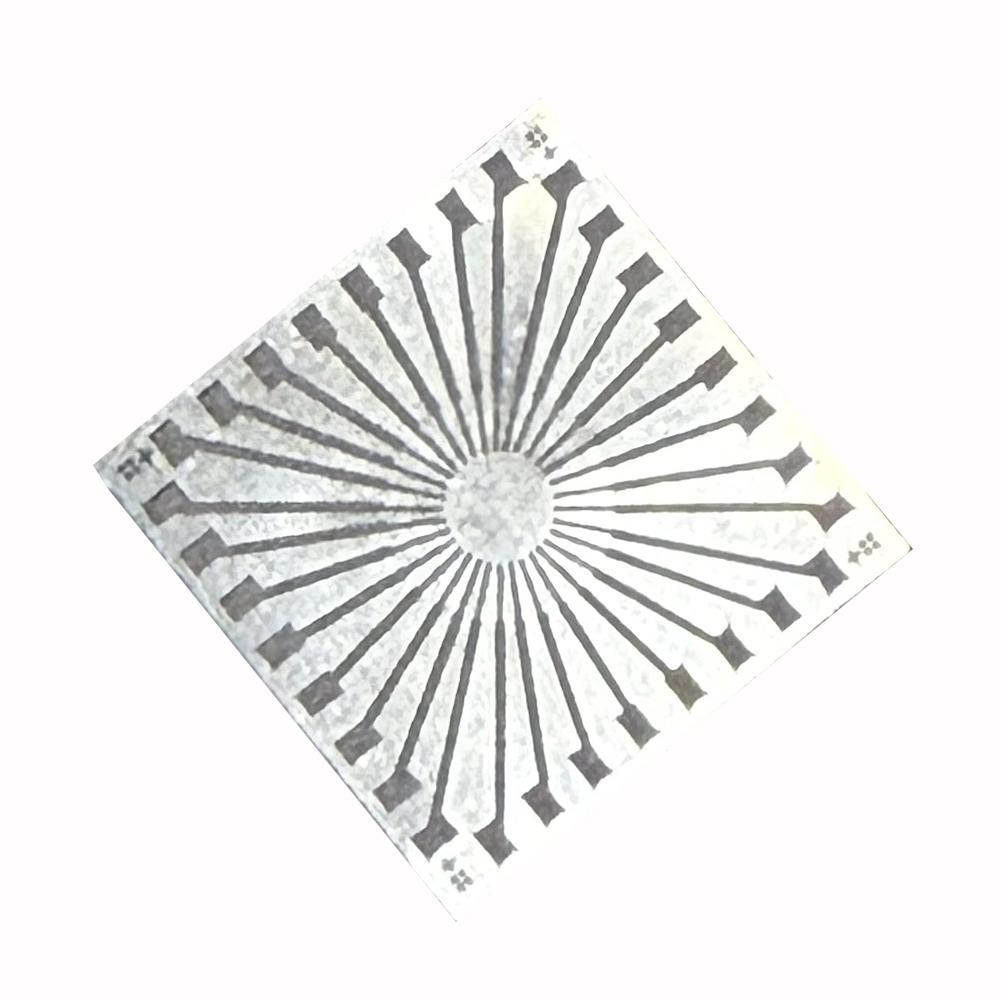
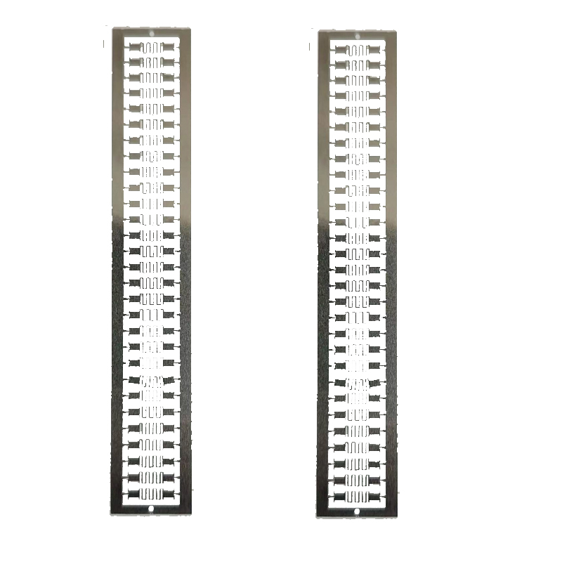
At YMJ Optical, we manufacture high‑precision laser‑cut stencils from your PCB Gerber layer files. Our stencils feature smooth, burr‑free apertures with straight wall profiles — optimising solder paste transfer volumes and placement positioning.
What Are Frameless Stencils?
Frameless stencils are stencils that can be used with or without a reusable frame or tensioning system. Unlike traditional framed stencils that are permanently glued to a metal frame, frameless stencils offer:
Lower cost — no frame or permanent adhesive required
Flexibility — interchangeable for different PCB assemblies
Easy storage — flat, stackable design
Rapid changeover — ideal for prototyping and low‑volume production
Compatibility — works with both framed and tensioning systems
Frameless stencils are available in a variety of materials, thicknesses, and aperture configurations to suit different applications.
Material Options for Frameless Stencils
Material Best For Key Characteristics
Stainless Steel High‑volume SMT production, fine‑pitch components Durable, wear‑resistant, excellent paste release, tight tolerances
Mylar (PET) Low‑cost, disposable, PCB rework Flexible, adhesive‑backed option, manual alignment
Kapton (Polyimide) High‑temperature applications, rework Heat‑resistant, flexible, adhesive‑backed
Other non‑metals Simple masking, short‑run prototyping Economical, easy to laser‑cut
Stainless Steel Stencils: Precision for Production
Stainless steel stencils are the industry standard for high‑precision SMT printing. At YMJ Optical, we fabricate stainless steel stencils with thicknesses selected based on:
Optimal solder paste transfer volume — thicker stencils deposit more paste
Smallest feature size — finer apertures require thinner materials to ensure clean paste release
Our laser‑cut stainless steel stencils are precisely manufactured from your PCB’s Gerber layer files. The result:
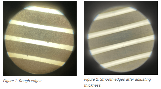
✅ Smooth apertures — free from burrs, raised edges, and debris
✅ Straight wall profiles — vertical aperture walls for consistent paste transfer
✅ Laser accuracy — tight tolerances for fine‑pitch components (0.4 mm pitch and below)
✅ Optimised transfer volumes — uniform paste deposition across the entire board
Wafer Stencils: Cost‑Effective Solder Bumping
Wafer stencils are an economical method for screening solder bumps onto an IC die (integrated circuit die) — a process known as wafer‑level bumping.
YMJ Optical’s laser‑cut wafer stencils accurately locate tens of thousands of the smallest apertures across a metallised wafer surface. With optimised laser processing:
Reduced heat‑affected areas — minimise thickness variations across the wafer
Consistent bump heights — uniform apertures result in uniform solder deposits
High‑density patterns — support advanced packaging (Flip Chip, WLCSP, Fan‑Out)
Flexible / Disposable Stencils: Cost‑Effective for Rework & Prototyping
For applications where cost or disposability is a priority, we offer frameless stencils made from Mylar (PET), Kapton (polyimide), and other non‑metal materials.
These flexible stencils are ideal for:
PCB rework — localised paste application for component replacement
Simple masking — temporary masking during assembly or coating
Low‑volume prototyping — cost‑effective alternative to stainless steel
Manual alignment — adhesive‑backed versions allow easy positioning and removal
Laser Cutting Advantages for Stencil Fabrication
YMJ Optical uses high‑precision laser cutting to manufacture all our stencils. Key advantages over chemical etching or electroforming:
Parameter Chemical Etching YMJ Laser Cutting
Aperture Tolerance ±25–50 µm ±12.7 µm (±0.0005″)
Edge Quality Tapered, undercut Straight, vertical, burr‑free
Minimum Cut Width 75–100 µm 25 µm (0.001″)
Material Thickness Range Limited 0.05 mm – 0.50 mm (flexible)
Tooling / Mask Cost High upfront No tooling cost
Design Change Cost New photo‑tool required Zero — update CAD/Gerber
Lead Time 2–4 weeks 3–5 days
Stencil Technical Specifications
Parameter YMJ Capability
Minimum Cut Width 0.001″ (25 µm)
Maximum Length 10 feet (3,048 mm) — material dependent
Maximum Width 30 inches (762 mm) — standard; larger available on request
Aperture Tolerance ±0.0005″ (±12.7 µm)
Materials Stainless steel, Mylar (PET), Kapton (polyimide), other non‑metals
Thickness Range 0.002″ – 0.020″ (0.05 mm – 0.50 mm)
Aperture Shape Round, square, rectangular, custom geometries
Edge Condition Burr‑free, no raised edges
Frameless Design Yes — compatible with reusable frames or tensioning systems
Applications
SMT assembly — solder paste printing for PCBs
Wafer bumping — solder bump screening for IC dies
Flip Chip packaging — fine‑pitch bumping
LED assembly — high‑density LED arrays
PCB rework — localised paste/flux application
Prototyping — fast‑turn, no‑tooling stencils
High‑volume production — durable stainless steel stencils
Why Choose YMJ Optical for Frameless Stencils?
Criterion YMJ Advantage
Precision ±0.0005″ aperture tolerance for fine‑pitch components
Edge Quality Burr‑free, straight walls for optimal paste release
Material Flexibility Stainless steel, Mylar, Kapton, and more
No Tooling Direct‑from‑Gerber fabrication — no photo‑tool costs
Fast Turnaround 3–5 business days for most stencils
Scalability Prototype, low‑volume, and high‑volume production
Expertise Years of laser micromachining for electronics manufacturing
How to Order: Simple 3‑Step Process
Step 1 – Submit Your Gerber Files
We require the following layers: solder paste, soldermask, silkscreen, and outline. Include your preferred thickness and material.
Step 2 – Design Confirmation
We generate a visual preview of your stencil showing all apertures. You approve or request changes.
Step 3 – Laser Cutting & Delivery
We laser‑cut your stencil, inspect for accuracy, and ship within the agreed lead time.
Frequently Asked Questions (FAQ)
Q1: What is the difference between a framed and frameless stencil?
A: A framed stencil is permanently mounted to a metal frame with adhesive. A frameless stencil can be used with or without a reusable frame or tensioning system, offering greater flexibility and lower cost.
Q2: What thickness should I choose for my stencil?
A: Thickness is determined by your smallest aperture and required solder paste volume. Typical thicknesses range from 0.004″ (for fine‑pitch) to 0.008″ (for standard components). We can recommend based on your Gerber file.
Q3: Can you make stencils for prototype quantities?
A: Yes. No minimum order quantity. We serve R&D labs, prototype shops, and high‑volume production lines equally.
Q4: What materials are available for frameless stencils?
A: Stainless steel (standard), Mylar (PET), Kapton (polyimide), and other non‑metal materials for disposable or rework applications.
Q5: Do you offer adhesive‑backed flexible stencils?
A: Yes. Mylar and Kapton stencils can be supplied with an adhesive backing for manual alignment and easy removal.
Q6: What is the typical lead time for a stencil?
A: 3–5 business days for standard stainless steel stencils. Expedited 24‑48 hour service is available for urgent projects.
Q7: What aperture tolerance do you guarantee?
A: ±0.0005″ (±12.7 µm) — industry‑leading precision for fine‑pitch SMT components.
Q8: Can you make stencils for wafer bumping?
A: Yes. We fabricate wafer stencils with tens of thousands of apertures across metallised surfaces for solder bump screening.